Twisted Bilayer MoS2 Band Structure
1. Introduction
This tutorial calculates the electronic band structure and the band gaps of the twisted bilayer molybdenum disulfide (MoS2) structures created in the structure creation tutorial, reproducing the electronic-structure result of the following manuscript.
Manuscript
Kaihui Liu, Liming Zhang, Ting Cao, Chenhao Jin, Diana Qiu, Qin Zhou, Alex Zettl, Peidong Yang, Steve G. Louie & Feng Wang, "Evolution of interlayer coupling in twisted molybdenum disulfide bilayers" Nature Communications volume 5, Article number: 4966 (2014) DOI: 10.1038/ncomms5966 1
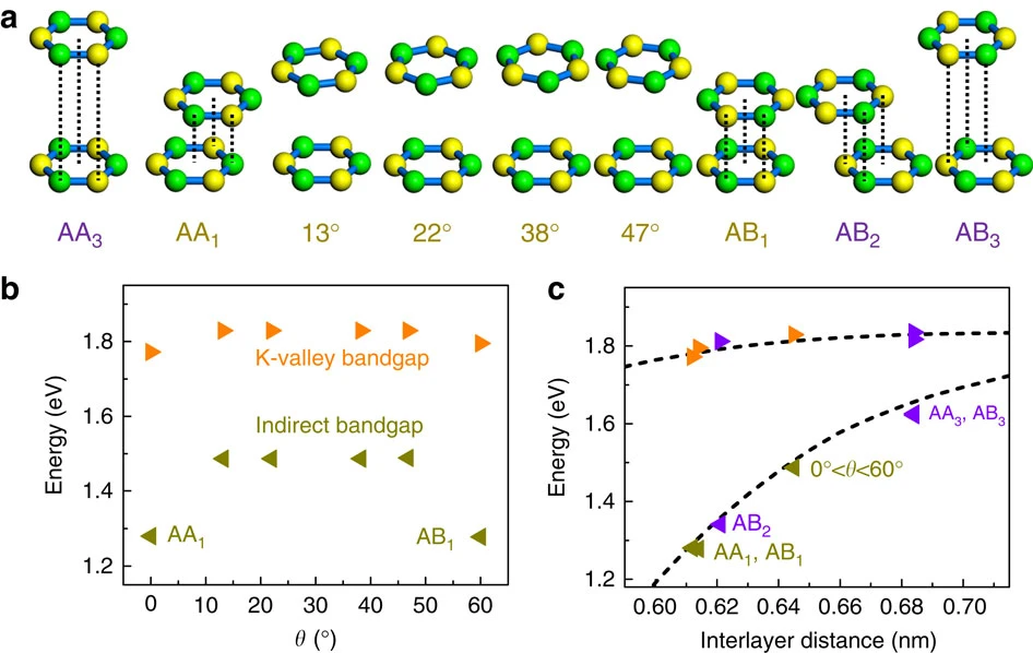
1.1. What the manuscript found
A MoS2 bilayer has an indirect bandgap, between a valence maximum at Γ and a conduction minimum at or near K. Both of those states are built from orbitals that stick out of the layer, so the size of the indirect gap measures how strongly the two layers are coupled; the K-valley states are confined within a layer and barely notice it.
The manuscript's result is that this coupling is set by the interlayer distance and nothing else:
- registered AA and AB stacking lets the two layers sit close together, and the indirect gap is markedly smaller there;
- every intermediate twist angle forces them apart by roughly the same amount — the sulfur atoms of the two layers can no longer interleave — and every twisted configuration lands on the same, larger indirect gap;
- the K-valley direct gap moves by around 0.02 eV across the entire range;
- horizontal alignment plays no part beyond setting the distance. Two bilayers at the same interlayer distance have the same indirect gap whether they are twisted or registered.
So the mechanism is steric rather than electronic: twisting changes the gap by changing how far apart the layers can sit.
1.2. Theory and experiment are different numbers
The manuscript reports photoluminescence peaks as well as calculated gaps, and these are not the same quantity. Photoluminescence measures optical transition energies, which include the binding energy of the exciton; a DFT calculation produces Kohn-Sham eigenvalue differences, which do not. The manuscript makes the point itself: the Kohn-Sham bandgaps should not be compared directly with the measured optical bandgaps, but the trend with twist angle should be correct.
This tutorial reproduces the trend, not the photoluminescence peaks.
2. Prerequisites
Run the
structure creation tutorial
first. Its notebook saves each structure it builds into the uploads folder under a name such as
MoS2 bilayer 21.8deg d6.5, and this notebook loads them back by exactly those names. A name that
does not resolve stops the notebook rather than silently substituting a different material.
3. What is calculated
One job per structure, all with the same settings, so the results can be compared with each other. The structure notebook builds the manuscript's configurations:
| structure | twist | d(Mo–Mo) | atoms |
|---|---|---|---|
MoS2 bilayer 21.8deg d6.5 |
21.8° | 6.5 Å | 42 |
MoS2 bilayer AB1 d6.1 |
60° | 6.1 Å | 6 |
MoS2 bilayer AB1 d6.5 |
60° | 6.5 Å | 6 |
MoS2 bilayer AA3 d6.8 |
0° | 6.8 Å | 6 |
MoS2 bilayer 13.2deg d6.5 |
13.2° | 6.5 Å | 114 |
MoS2 bilayer 38.2deg d6.5 |
38.2° | 6.5 Å | 42 |
MoS2 bilayer 46.8deg d6.5 |
46.8° | 6.5 Å | 114 |
MoS2 bilayer AB1 d6.5 is not one of the manuscript's own configurations — it is the registered
stacking held at the twisted structures' interlayer distance, which separates the effect of the
distance from the effect of the horizontal alignment.
The simulation notebook computes the first entry by default; uncomment the others to add them. The 114-atom cells are considerably more expensive than the rest.
3.1. Interlayer distances are inputs here, not outputs
The distances above are the manuscript's Table S1 LDA values — the relaxed results of its own calculations. This tutorial builds the structures at those distances and does not relax them.
The structure notebook prints the Mo–Mo separation of each finished structure next to the value it was aiming for, along with the cell height, so the geometry can be checked against the manuscript at a glance.
3.2. Which registry a 0° or 60° stack comes out as
Registered stacking is not a single structure. The manuscript distinguishes sulfur over molybdenum (AA1, AB1), sulfur over the centre of a hexagon (AA2, AB2) and sulfur over sulfur (AA3, AB3), and Table S1 gives each a different interlayer distance — 6.1 Å, 6.2 Å and 6.8 Å respectively, the eclipsed S-over-S stacking being pushed furthest apart.
The structure builder has no registry parameter: it returns whatever the commensurate lattice search produces. The structure notebook therefore classifies each registered stack it builds from the in-plane offset between the facing sulfur planes and prints the answer. With the current builder, 0° produces AA3 and 60° produces AB1, which is why the 60° structure is the registered member of the comparison — it is the compact stacking the manuscript's headline sentence is about.
4. Calculation parameters
The manuscript used DFT in the local density approximation with norm-conserving pseudopotentials, a plane-wave cutoff of 140 Ry, 20 Å between periodic images along the out-of-plane direction, and no spin-orbit coupling.
| this tutorial | manuscript | |
|---|---|---|
| Functional | LDA (pz) |
LDA |
| Pseudopotentials | ultrasoft (GBRV) | norm-conserving |
| Wavefunction cutoff | 40 Ry, density 320 Ry | 140 Ry |
| Out-of-plane cell | 20 Å | 20 Å |
| Spin-orbit coupling | off | off |
| Spin polarization | off | not applicable |
| Geometry | interlayer distances from Table S1 | relaxed |
The pseudopotentials are the one real divergence, and it is forced: the platform carries no norm-conserving set for Mo or S under LDA, so the closest available match is the ultrasoft GBRV set at the same functional. Keeping the functional is what matters — LDA is what binds this bilayer.
The two cutoffs are not the same quantity. 140 Ry is a norm-conserving wavefunction cutoff; ultrasoft pseudopotentials converge the wavefunctions far lower and instead need a charge-density cutoff eight to twelve times higher, which is the 320 Ry here.
Expect absolute gaps roughly 0.2 eV below the manuscript's as a result. Differences between structures computed with identical settings are much less affected, and those carry the result.
4.1. K-point sampling and cell size
The k-grid is set per structure, alongside its name:
1 2 3 4 5 | |
The manuscript does not state its k-sampling. A commensurate supercell has a Brillouin zone smaller
by its cell count, so it needs fewer divisions than the 1×1 cell for equivalent sampling — hence
[6, 6, 1] for the √7×√7 cell against [12, 12, 1] for the 1×1.
Keep the in-plane divisions a multiple of three. K sits at (1/3, 1/3), so a Γ-centred grid whose divisions are not divisible by three never samples it, and the K-valley gap is then read at some other k-point.
4.2. The band structure path belongs to the cell being computed
The path is Γ–M–K–Γ of whichever cell is being calculated. In a supercell the bands are folded onto
a smaller Brillouin zone, so the point labelled K in the 42-atom plot is not the K point of the
monolayer. The plots are for reading; the numbers the comparison uses come from the band_gaps
property, which is extracted from the non-self-consistent k-mesh and is unaffected by folding.
5. Step-by-step instructions
5.1. Create the structures
Run the
structure creation notebook.
Its INTERFACE_PARAMETERS list has the three structures compared here active by default —
building a structure costs seconds, so there is no reason to build fewer. Uncomment further entries
for the remaining twist angles.
5.2. Open the simulation notebook
1 | |
5.3. Select the materials
Cell 1.2 holds the structures to compute and the k-grid for each:
1 2 3 4 5 6 | |
One job is created per entry. Uncomment the two AB1 entries to run the full comparison.
5.4. Run the notebook
Select Run > Run All. The notebook will authenticate with the platform, load and save the materials, build one workflow per material, create and submit one job each, wait for them, and then print the results.
The 42-atom job dominates the cost. Raising PPN or moving to a larger queue is the sensible lever;
reducing INTERFACE_VACUUM in the structure notebook is the other one, though it should not go
below the manuscript's ≈ 10 Å of vacuum, and it has to be the same for every job in the comparison.
6. Expected results
6.1. Gaps against twist angle
Each structure produces one row, and the notebook plots the indirect and K-valley direct gaps against twist angle — the same axes as Fig. 4b of the manuscript. Alongside each row it shows the manuscript's own value, read off that figure: about 1.27 eV for the registered AB stacking, 1.47 eV for every twist, 1.60 eV for the eclipsed AA stacking, and a K-valley gap near 1.80 eV throughout.
Absolute gaps come out roughly 0.2 eV below the manuscript's, because the pseudopotentials are not its norm-conserving set. Differences between structures computed with identical settings are much less affected, and those are what carry the manuscript's claim.
Measured on two structures that differ only in interlayer distance:
| structure | d(Mo–Mo) | indirect | direct (K) |
|---|---|---|---|
MoS2 bilayer AB1 d6.1 |
6.1 Å | 1.098 eV | 1.612 eV |
MoS2 bilayer AB1 d6.5 |
6.5 Å | 1.297 eV | 1.624 eV |
The indirect gap shifts +0.199 eV over that 0.4 Å, against +0.20 eV in Fig. 4c, while the K-valley gap moves 0.012 eV — the manuscript's result, that the indirect gap tracks the interlayer distance and the K-valley gap does not.
6.2. Band structure
Each job produces a band structure along Γ–M–K–Γ of its own cell. A supercell's bands are folded onto its smaller Brillouin zone, so it carries proportionally more bands over a smaller range — the same electronic structure, drawn differently.
7. Troubleshooting
The comparison at the same interlayer distance is the one sensitive to k-point sampling, because it is the only one between cells of different size. If it disagrees while the others hold, check that the supercell's grid is scaled down relative to the 1×1 cell's as described in 4.1.
If every gap is far from 1.5 eV, check the interlayer distance printed for each material against the value in its name before looking anywhere else.
8. Interactive JupyterLite notebook
The notebook below calculates the band structures and evaluates the comparison. Select Run > Run All Cells.
9. References
-
Kaihui Liu, Liming Zhang, Ting Cao, Chenhao Jin, Diana Qiu, Qin Zhou, Alex Zettl, Peidong Yang, Steve G. Louie, and Feng Wang. Evolution of interlayer coupling in twisted molybdenum disulfide bilayers. Nature Communications, 5:4966, 2014. URL: https://doi.org/10.1038/ncomms5966, doi:10.1038/ncomms5966. ↩